The semiconductor industry is an important sector that is currently experiencing a lot of growth with the increasing demand for electronic devices. As the need for more advanced and sophisticated electronic devices continues to grow, the semiconductor industry is constantly looking for new and improved ways of producing these devices.
One of the key areas of focus for the semiconductor industry is the use of sputtering targets and deposition materials. Sputtering targets are materials that are used in a process known as sputtering to deposit thin films onto a substrate. Deposition materials, on the other hand, are materials that are used in various deposition processes to create thin films of a particular material.
Sputtering targets and deposition materials have a wide range of benefits when used in the semiconductor industry. These benefits include:
1. Improved efficiency
One of the main benefits of using sputtering targets and deposition materials in the semiconductor industry is improved efficiency. Sputtering targets and deposition materials are highly efficient in the deposition of thin films onto a substrate, which in turn results in the production of electronic devices that have better performance and reliability.
2. Enhanced quality
Sputtering targets and deposition materials are also known to enhance the quality of electronic devices. By ensuring that the deposition process is accurate and precise, sputtering targets and deposition materials help to produce electronic devices of high quality and consistency.
3. Cost-effectiveness
Another benefit of using sputtering targets and deposition materials is cost-effectiveness. Sputtering targets and deposition materials are highly durable and long-lasting, which means that they need to be replaced less frequently. This, in turn, helps to reduce the overall cost of production in the semiconductor industry.
4. Improved productivity
In addition to improving efficiency, quality, and cost-effectiveness, sputtering targets and deposition materials also help to improve productivity in the semiconductor industry. By reducing downtime and increasing production output, sputtering targets and deposition materials help to ensure that the industry meets the increasing demand for electronic devices.
Overall, the semiconductor industry can benefit significantly from the use of sputtering targets and deposition materials. With the help of these materials, the industry can produce electronic devices of higher quality, efficiency, and performance, while also reducing the overall cost of production.
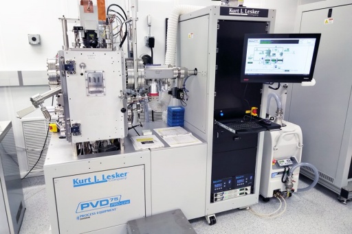
Xiangtan Hondson Coating Technology Co., Ltd. is a company that specializes in the manufacture of Physical Vapor Deposition (PVD) systems. Their range of sputtering targets and deposition materials, including gold, titanium-aluminum, vanadium, molybdenum, and niobium targets, are highly effective in the production of electronic devices.
With engineering excellence, quality, and reliability as their primary values, Xiangtan Hondson Coating Technology Co., Ltd. is a company that can be trusted to deliver high-quality sputtering targets and deposition materials that meet the needs of the semiconductor industry.
In conclusion, the semiconductor industry is a crucial sector that requires innovative and reliable solutions to keep up with the increasing demand for electronic devices. Sputtering targets and deposition materials provide a highly effective solution for the production of high-quality, efficient, and cost-effective electronic devices. With the help of companies like Xiangtan Hondson Coating Technology Co., Ltd., the semiconductor industry can continue to thrive and meet the needs of consumers worldwide.